- 您现在的位置:买卖IC网 > Sheet目录336 > KIT34712EPEVBE (Freescale Semiconductor)KIT EVAL BOARD 3A 1MHZ
�� �
�
�PIN� CONNECTIONS�
�PIN� CONNECTIONS�
�24�
�23�
�22�
�21�
�20�
�19�
�GND�
�1�
�18� PVIN�
�FREQ�
�2�
�17�
�SW�
�NC�
�PG�
�3�
�4�
�Transparent�
�Top� View�
�PIN� 25�
�16�
�15�
�SW�
�SW�
�STBY�
�5�
�14� PGND�
�SD�
�6�
�13�
�PGND�
�7�
�8�
�9�
�10�
�11�
�12�
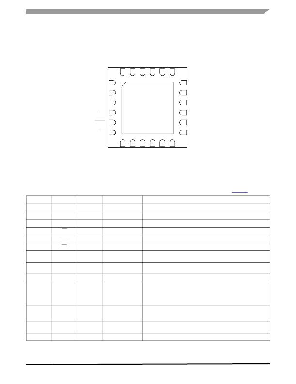
�Figure� 3.� 34712� Pin� Connections�
�Table� 1.� 34712� Pin� Definitions�
�A� functional� description� of� each� pin� can� be� found� in� the� Functional� Pin� Description� section� beginning� on� page� 10� .�
�Pin� Number�
�1�
�Pin� Name�
�GND�
�Pin� Function�
�Ground�
�Formal� Name�
�Signal� Ground�
�Analog� signal� ground� of� IC�
�Definition�
�2�
�FREQ�
�Passive�
�Frequency� Adjustment� Buck� converter� switching� frequency� adjustment� pin�
�3�
�4�
�5�
�6�
�7�
�8�
�9�
�10�
�11�
�12,13,14�
�15,16,17�
�18,19,20�
�21�
�NC�
�PG�
�STBY�
�SD�
�VREFIN�
�VREFOUT�
�COMP�
�INV�
�VOUT�
�PGND�
�SW�
�PVIN�
�BOOT�
�None�
�Output�
�Input�
�Input�
�Input�
�Output�
�Passive�
�Input�
�Output�
�Ground�
�Output�
�Supply�
�Passive�
�No� Connect�
�Power� Good�
�Standby�
�Shutdown�
�Voltage� Tracking�
�Reference� Input�
�Reference� Voltage�
�Output�
�Compensation�
�Error� Amplifier�
�Inverting� Input�
�Output� Voltage�
�Discharge� FET�
�Power� Ground�
�Switching� Node�
�Power-circuit� Supply�
�Input�
�Bootstrap�
�No� internal� connections� to� this� pin�
�Active-low� (open� drain)� power-good� status� reporting� pin�
�Standby� mode� input� control� pin�
�Shutdown� mode� input� control� pin�
�Voltage� tracking� reference� voltage� input�
�Buffered� output� equal� to� 1/2� of� voltage-tracking� reference�
�Buck� converter� external� compensation� network� pin�
�Buck� converter� error� amplifier� inverting� input� pin�
�Discharge� FET� drain� connection� (connect� to� buck� converter� output�
�capacitors)�
�Ground� return� for� buck� converter� and� discharge� FET�
�Buck� converter� power� switching� node�
�Buck� converter� main� supply� voltage� input�
�Bootstrap� switching� node� (connect� to� bootstrap� capacitor)�
�34712�
�Analog� Integrated� Circuit� Device� Data� ?�
�Freescale� Semiconductor�
�3�
�发布紧急采购,3分钟左右您将得到回复。
相关PDF资料
KIT34713EPEVBE
KIT EVAL BOARD 5A 1MHZ
KIT34716EPEVBE
KIT EVAL BOARD 1MHZ DUAL SW-MODE
KIT34717EPEVBE
KIT EVAL BOARD 5A 1.0MHZ
KS-1787-MG
SHELF SLIDING KEYBOARD ASSEMBLY
KS-1788
SHELF SLIDING KEYBOARD ASSEMBLY
KSDKSTM32-PL
KIT IAR KICKSTART STM32 CORTEXM3
LC4064ZC-EV
BOARD EVAL FOR ISPMACH 4064ZC
LCMXO2280C-C-EVN
BOARD CONTROL EVAL MACHXO
相关代理商/技术参数
KIT34713EPEVBE
功能描述:电源管理IC开发工具 5.0 A 1.0 MHZ FULLY INTEG RoHS:否 制造商:Maxim Integrated 产品:Evaluation Kits 类型:Battery Management 工具用于评估:MAX17710GB 输入电压: 输出电压:1.8 V
KIT34716EPEVBE
功能描述:电源管理IC开发工具 1.0 MHZ DUAL SWITCH-MODE RoHS:否 制造商:Maxim Integrated 产品:Evaluation Kits 类型:Battery Management 工具用于评估:MAX17710GB 输入电压: 输出电压:1.8 V
KIT34717EPEVBE
功能描述:电源管理IC开发工具 5.0 A 1.0MHZ FULLY INTEG RoHS:否 制造商:Maxim Integrated 产品:Evaluation Kits 类型:Battery Management 工具用于评估:MAX17710GB 输入电压: 输出电压:1.8 V
KIT34727FCEVBE
功能描述:电源管理IC开发工具 600MA HIGH EFFICIENCY LO RoHS:否 制造商:Maxim Integrated 产品:Evaluation Kits 类型:Battery Management 工具用于评估:MAX17710GB 输入电压: 输出电压:1.8 V
KIT34825EPEVME
功能描述:界面开发工具 MICRO USB INTERFACE IC RoHS:否 制造商:Bourns 产品:Evaluation Boards 类型:RS-485 工具用于评估:ADM3485E 接口类型:RS-485 工作电源电压:3.3 V
KIT34844AEPEVBE
功能描述:LED 照明开发工具 IC, 10 CHANNEL LED BACKLIGHT RoHS:否 制造商:Fairchild Semiconductor 产品:Evaluation Kits 用于:FL7732 核心: 电源电压:120V 系列: 封装:
KIT34844EPEVME
功能描述:LED 照明开发工具 MC34844 10-Ch LED BL Driver Eval Kit
RoHS:否 制造商:Fairchild Semiconductor 产品:Evaluation Kits 用于:FL7732 核心: 电源电压:120V 系列: 封装:
KIT34845EPEVME
功能描述:LED 照明开发工具 IC, 6 CHANNEL LED BACKL RoHS:否 制造商:Fairchild Semiconductor 产品:Evaluation Kits 用于:FL7732 核心: 电源电压:120V 系列: 封装: